
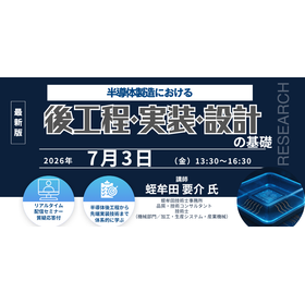
7/3 Webinar on Backend Processes, Assembly, and Design in Semiconductor Manufacturing
A systematic explanation from the basics of semiconductor backend processes and packaging technology to 2.5D/3D packaging and chiplet technology.
■Title "Fundamentals of Backend Processes, Packaging, and Design in Semiconductor Manufacturing" This seminar provides a systematic learning experience about backend processes and packaging technologies that support the high performance and functionality of semiconductors, covering everything from the basics to the latest trends. Experienced instructors will clearly explain the history of semiconductor package evolution, various package types, packaging processes, encapsulation technologies, and evaluation and analysis techniques. Additionally, the latest trends in advanced packaging technologies such as 2.5D/3D packaging, CoWoS, chiplets, hybrid bonding, and optoelectronic integration technologies that support the AI era will also be introduced. This content is recommended for engineers and researchers in fields such as chemistry, electronic components, and the automotive industry, as well as anyone who wants to learn semiconductor packaging technology from the ground up.
- Company:CMC RESEARCH Ltd.
- Price:Other
